
Electronics and Communication Engineering Questions and Answers
Prepare for your Electronics and Communication Engineering exams/aptitude tests, assess your knowledge of electronics and communication equipment with these ECE questions and answers.
Prepare for your Electronics and Communication Engineering exams/aptitude tests, assess your knowledge of electronics and communication equipment with these ECE questions and answers.
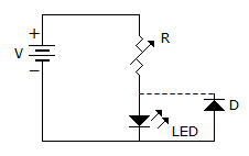
In the circuit above, the function of resistor R and diode D are
to limit the current and to protect LED against over voltage
to limit the voltage and to protect LED against over current
to limit the current and protect LED against reverse breakdown voltage.
none of the above.
Correct answer is C
Resistance limits current and diode is reverse connected and therefore protects LED against reverse breakdown.
Assertion (A): A p-n junction has high resistance in reverse direction.
Reason (R): When a reverse bias is applied to p-n junction, the width of depletion layer increases.
Both A and R are true and R is correct explanation of A
Both A and R are true but R is not a correct explanation of A
A is true but R is false
A is false but R is true
Correct answer is A
The increase in reverse resistance is due to widening of depletion layer.
The amount of photoelectric emission current depends on
frequency of incident radiation
intensity of incident radiation
both frequency and intensity of incident radiation
none of the above
Correct answer is B
Only the intensity of incident radiation governs the amount of photoelectric emission.
In an n channel JFET, the gate is
n type
p type
either n or p
partially n & partially p
Correct answer is B
Since channel is n type gate must be p type.
A transistor has a current gain of 0.99 in the CB mode. Its current gain in the CC mode is
100
99
1.01
0.99
Correct answer is A
β = (α / 1 - α) ⇒ (0.99 / 1 - 0.99) = 99 ⇒ Current gain = 1 + β = 100
In which of these is reverse recovery time nearly zero?
Zener diode
Tunnel diode
Schottky diode
PIN diode
Correct answer is C
In schottky diode there is no charge storage and hence almost zero reverse recovery time.
The most commonly used semiconductor material is
silicon
germanium
mixture of silicon and germanium
none of the above
Correct answer is A
Germanium is rarely used
At room temperature, the current in an intrinsic semiconductor is due to
holes
electrons
ions
holes and electrons
Correct answer is D
Intrinsic material has equal number of holes and electrons.
Programme Officer at the International Fund for Agricultural Development (IFAD)
Customer Relations Officer at Abuja Electricity Distribution Company (AEDC Plc)
Administrative Assistant at Five Thousand Miles
Human Resources Officer at Boctrust Microfinance Bank
Content Creator / Graphic Designer / Video Editor at Marriott International
Corporate Finance Analyst at Radix Capital Partners Limited
Assistant HR Officer at MacTay Consulting